
Key points
- Edinburgh Worldwide is finding AI opportunities beyond headline chip makers as computing systems grow more complex
- The portfolio’s semiconductor holdings span testing, connectivity and packaging, where new bottlenecks can create value
- BESI and Shibaura reflect the managers’ broader view that solving system complexity may matter more than backing one winner
As with any investment, your capital is at risk.
So far, the most visible stars of the AI boom are the cutting-edge large language models, powered by NVIDIA. But the vast datacentres behind Claude and ChatGPT don’t house only chips.
They are complex systems of memory, switches, connections and power management, all working in harmony with those NVIDIA chips. As AI models grow, the bottleneck increasingly becomes not just the computing power available, but how efficiently these systems work together.
The scale of the opportunity is hard to ignore. Earlier this year, estimates suggested that the major cloud providers would spend around $650bn in 2026, much of it directed toward AI infrastructure. Following this quarter’s earnings, that figure has moved above $700bn. And this only captures the largest listed cloud platforms. It excludes other sources of demand, such as big businesses like Oracle, newer cloud providers, and government projects.
AI is now among the greatest infrastructure builds in history, and it is pulling on every part of the semiconductor supply chain: graphics processing units (GPUs), memory, networking, power, cooling, testing and, increasingly, advanced packaging.
That matters for Edinburgh Worldwide. Over the last two years, the portfolio’s exposure to semiconductors and related equipment has increased significantly. This is not a single bet on AI, nor a top-down call to own more ‘chip stocks’. It reflects a broader view: as demand for computing power rises, the most interesting opportunities may sit in the less visible parts of the semiconductor industry.
The problem: Moore’s law is changing
For decades, semiconductor progress was driven by Moore’s law: if transistors kept getting smaller, more of them fit onto the same piece of silicon and performance improved. That is no longer a certainty. It is now more difficult, expensive, and can’t be relied upon to deliver the next wave of increased computing performance.
Today, the bottleneck is not only how fast a chip can run. It is how quickly memory can feed it data. A modern AI processor can perform trillions of operations per second, but only if data is available at the right time. If the data sits too far away, the processor waits. Computing power has improved far faster than memory, so moving data efficiently is now a central challenge in chip design. How do you make many separate pieces of silicon behave like a single efficient system?
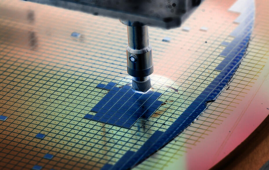
The answer to this challenge is not one technology, but multiple solutions. One is advanced packaging – a semiconductor manufacturing technique that allows multiple chips to be ‘packaged’ together to improve speed and efficiency.
Packaging used to mean protecting a chip from moisture, contamination and physical damage. Today, it is increasingly about performance. If data cannot move quickly enough between the processor and memory, the system slows. If heat cannot be managed, the system underperforms. If the connections between chips are not dense or reliable enough, the architecture fails.
This is typified by ‘CoWoS’, short for chip-on-wafer-on-substrate. In simple terms, it’s chip builder TSMC’s way of bringing the processor and memory much closer together. Traditional systems can force data to travel across centimetres of circuit board. CoWoS places the logic chip and memory stacks on a shared silicon interface, reducing that distance to micrometres. The result is much faster-moving data and lower energy use. For AI datacenters, where GPUs constantly need to pull information from memory, that distance matters.
This might be technical, but the investment point is simple. The more computing power grows, the more the bottleneck moves from the chip itself to the system around it: how chips are connected, powered and cooled.
Why technical understanding matters
You don’t have to look far for semiconductor analysis today. AI-related stocks have jumped sharply, and any possible bottleneck is combed over by everyone from sell-side analysts and industry bloggers to Reddit users debating the finer points with surprising intensity.
In a crowded trade, the investment question is not simply whether AI grows. There is little edge in saying AI needs more chips. The harder, more insightful, question is where will value migrate as the system becomes constrained? Value often accrues to the layer that becomes unavoidable: the point every system must pass through, which cannot be quickly replicated, and where customers have little choice but to pay for high performance.
Today, that bottleneck may be GPU supply. Tomorrow, it may be high-bandwidth memory. Beyond that, we are looking at advanced packaging capacity, CoWoS and other solutions like hybrid bonding yields, thermal dissipation, testing intensity, power delivery or something else entirely. A process that looks obscure today can become strategically important very quickly.
That is why we spend time understanding the technical direction of travel. If we are not simply to own the most visible winner of the current cycle, we must take a view on which engineering challenges are becoming more important, which suppliers are genuinely differentiated, and where the market may be underestimating the durability or size of the opportunity.
Not every bottleneck is an attractive equity investment. Some are too capital-intensive, too slow-growing, or already fully recognised by the market. Our task is to find the points where technical importance, growth, competitive advantage and valuation overlap.
That brings us to two companies we purchased in April: BESI and Shibaura Mechatronics.
BESI: bonding chips together
BESI is a Dutch semiconductor equipment company. In crude terms, it makes machines that stick semiconductor modules together. That massively undersells the difficulty. At the leading edge, ‘sticking chips together’ now requires atomic-level precision, cleanliness and process control.
BESI is the leader in hybrid bonding, a next-generation packaging technology that eliminates solder and creates direct copper-to-copper connections between chips. These connections can be far denser than traditional approaches, enabling faster data movement and improved thermal performance. In effect, hybrid bonding helps separate silicon pieces, so they behave more like a single larger chip.
That is potentially powerful. If traditional transistor scaling, predicted by Moore’s law, is becoming harder, then stacking and connecting chips more intelligently becomes one of the most attractive paths to continued performance gains. Hybrid bonding may be used in high-performance logic, high-bandwidth memory, co-packaged optics and eventually mobile processors. It is not the only path forward, but it is one of the most compelling.
The appeal of BESI is that it offers a relatively pure expression of this shift. It is already a leader in advanced die placement, has a strong position in hybrid bonding and benefits from a partnership with Applied Materials, which helps provide an integrated solution around surface preparation, cleaning, metrology and bonding.
This is not an investment without risk – hybrid bonding adoption may be slower, narrower or more uneven than expected. It is, however, a high-quality business leading in a valuable area of technical transition. That is worthy of a place in the portfolio.
Shibaura: the understated alternative
Shibaura Mechatronics is a very different company. It is Japanese, more diverse, and less widely covered. Historically, it was associated with flat-panel display equipment, but over the last decade, it has repositioned itself as a supplier of critical semiconductor tools.
At first glance, Shibaura’s range of products looks disjointed. It spans diverse niches such as front-end cleaning and wet etching, photomask tools, flip-chip bonders and emerging hybrid bonding platforms. The common thread is technical skill: precision control under extremely tight cleanliness constraints.
That skill may become more valuable as the line between front-end manufacturing and back-end packaging blurs. Advanced packaging increasingly requires cleanliness and precision. Hybrid bonding, in particular, needs extremely flat, particle-free surfaces.
Shibaura already has experience in cleaning and has been working on hybrid bonding for several years. It may not be the technical leader today – BESI appears to hold that position – but it could become an important second source or find valuable niches where its ability to integrate cleaning and bonding matters.
Shibaura also has attractive exposure to CoWoS. Its TFC-6500 flip-chip bonder is used in the chip-on-wafer step for GPU packaging, precisely the kind of process that becomes more important as AI datacentres grow larger and more complex.
The contrast with BESI is useful. BESI is the clearer leader in hybrid bonding and the purer expression of that technology. Shibaura trades at a discount to peers in the sector, though its long-standing relationship with TSMC is a testament to its capabilities.
Owning both reflects our humility about the exact path advanced packaging will take, while expressing confidence that the importance and complexity of packaging will continue to rise.
A broader semiconductor exposure
BESI and Shibaura are the most recent examples, but they reflect a broader portfolio shift. Edinburgh Worldwide’s portfolio now includes other semiconductor-related stocks ASPEED, Aehr Test Systems, Astera Labs, Silergy, Impinj, and PDF Solutions.
These businesses do not all do the same thing, and that is the point. Astera Labs helps move data around AI datacentres, addressing the connectivity bottlenecks between processors, memory and storage.
Aehr Test Systems specialises in semiconductor testing and reliability. PDF Solutions helps manufacturers improve yield and process control. ASPEED, Silergy and Impinj provide exposure to specialist semiconductor niches, from server management chips to power management and connectivity. BESI and Shibaura now add advanced packaging and bonding equipment to that mix.
This is not a single-factor bet on one company, one customer or one AI architecture. We do not need to know exactly which chip design wins in 2030.
Rather, this collective positioning reflects our view that, as systems become more powerful, they also become more complex. Complexity tends to create bottlenecks. Bottlenecks create value for companies that can solve them.
Important information
This communication was produced and approved in June 2026 and has not been updated subsequently. It represents views held at the time of writing and may not reflect current thinking.
This article does not constitute, and is not subject to the protections afforded to, independent research. Baillie Gifford and its staff may have dealt in the investments concerned. The views expressed are not statements of fact and should not be considered as advice or a recommendation to buy, sell or hold a particular investment.
Baillie Gifford & Co and Baillie Gifford & Co Limited are authorised and regulated by the Financial Conduct Authority (FCA).
Some of the views expressed are not necessarily those of Baillie Gifford. Investment markets and conditions can change rapidly, therefore the views expressed should not be taken as statements of fact nor should reliance be placed on them when making investment decisions.
Baillie Gifford & Co and Baillie Gifford & Co Limited are authorised and regulated by the Financial Conduct Authority (FCA). The investment trusts managed by Baillie Gifford & Co Limited are listed on the London Stock Exchange and are not authorised or regulated by the FCA.
A Key Information Document is available at bailliegifford.com.